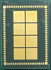
/filters:background_color(white)/2024-04/Sona%20TI351%20-%20Family%20%281%29.png)
Preface - PCNs
PCN #: 6K-2025
Date: June 13th, 2025
Products Affected
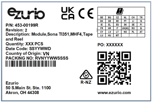
| Ezurio Part Number | Description |
| 453-00199R | Module, Sona TI351, MHF4, Tape and Reel |
| 453-00199C | Module, Sona TI351, MHF4, Cut Tape |
| 453-00200R | Module, Sona TI351, Integrated Antenna, Tape and Reel |
| 453-00200C | Module, Sona TI351, Integrated Antenna, Cut Tape |
| 453-00209 | Module, Sona TI351, M.2 2230 |
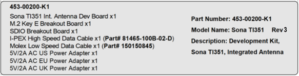
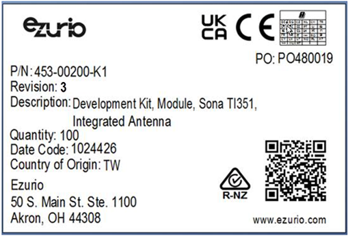
| 453-00200-K1 | Development Kit, Module, Sona TI351, Integrated Antenna |
Description of Changes
This change updates OTP content to incorporate the Ezurio MAC address and add Ezurio specific keys.
Devices prior to date code 1225361 are considered pre-production and are not supported.
Reason for Change
This change is necessary to secure regulatory related parameters for compliance and enable Ezurio specific firmware features in the future.
Anticipated Impact of the Change
This change has the following impact compared to the previous pre-production devices starting with the Ezurio 2025 Q2 software release (13.24.0.20) containing the Texas Instruments 1.0.2.9 release:
- MAC address is from an Ezurio pool instead of a Texas Instruments pool
- Regulatory related parameters in the configuration binary are protected against modification. Configuration binaries with modifications to protected parameters will fail to load.
- Enhanced Ezurio firmware will be supported when available in a future software release. Enhanced Ezurio firmware will fail to load on pre-production devices.
IMPORTANT: Pre-production devices will not be compatible with future software releases.
IMPORTANT: Pre-production software (prior to 13.24.0.20) does not support OTP configuration. Production devices based on this PCN running pre-production software prior to 13.24.0.20 will use a MAC address that does not match the Ezurio MAC address stamped on the TI351.
Method of Identifying the Changed Product
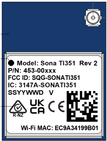
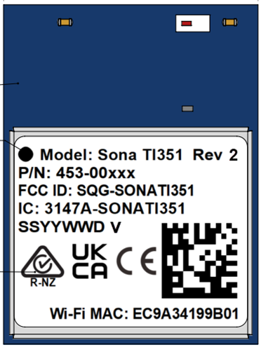
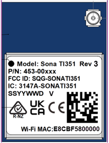
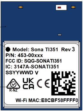
Update Label/Laser-etching
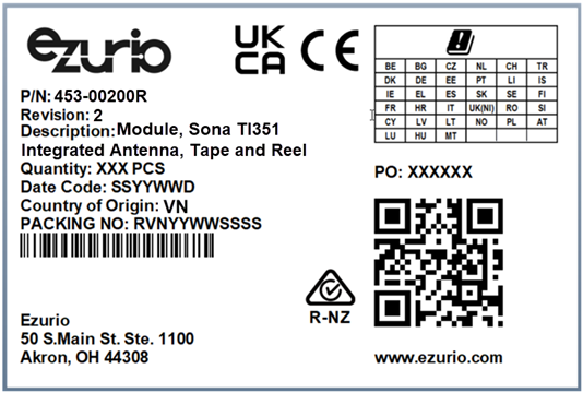
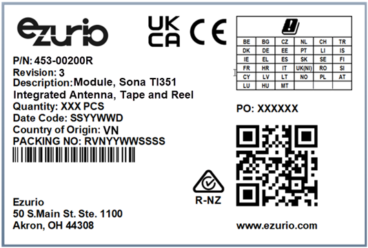
453-00199R, 453-00199C, 453-00200R, 453-00200C
On the module
- Update from labelling to laser-etching.
- Update the revision from Rev 2 to Rev 3.
On the packaging labels
- Update the revision from Rev 2 to Rev 3.
| BEFORE | AFTER |
  |   |
   |    |
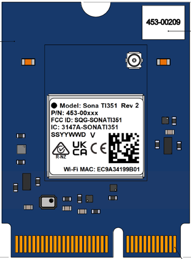
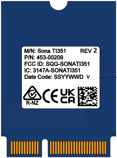
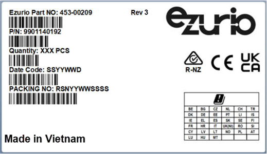
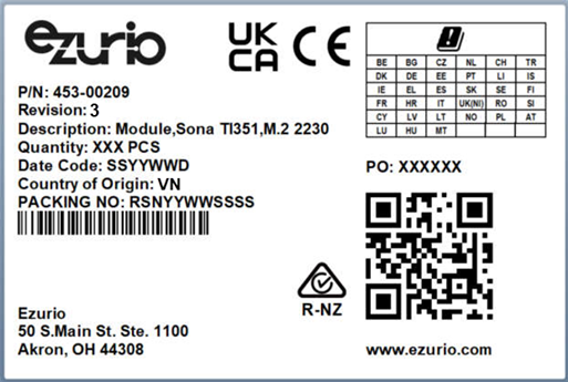
453-00209
- On the module laser-etching, change the revision from Rev 2 to Rev 3.
- On the back product label, change the revision from Rev 2 to Rev 3.
- On the packaging labels, change the revision from Rev 2 to Rev 3.
| BEFORE | AFTER |
  |   |
  |   |
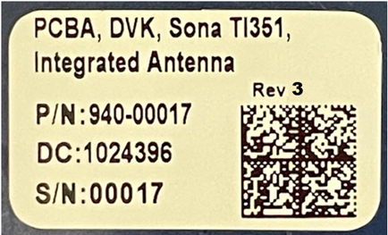
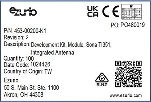
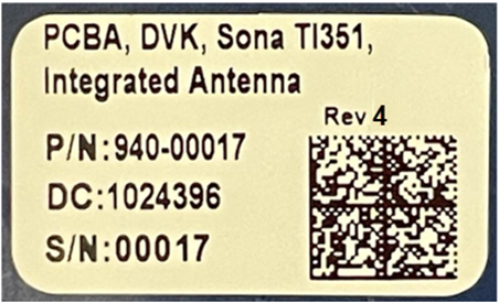
453-00200-K1
- On the module laser-etching, change the revision from Rev 2 to Rev 3.
- On the dev board PCBA label, change from Rev 3 to Rev 4.
- On the dev kit content label, change from Rev 2 to Rev 3.
- On the shipping label, change from Rev 2 to Rev 3.
| BEFORE | AFTER |
    |     |
Change Implementation
Factory Effective Date
These changes will be implemented into manufacturing starting from Date Codes, as outlined below for each product variant. The date code is shown on each label, as format SSYYWWD.
SS = Supplier code
YY = last two numbers of the year (ex: 18=2018, 19=2019)
WW = Week of the year
D = day of the week (ex: Sun=1, Mon=2, Tue=3, Wed=4, Thu=5, Fri=6, Sat=7)
| Ezurio Part Number | Factory Effectivity – Date Codes |
|---|---|
| 453-00199R | 1225361 |
| 453-00199C | 1225361 |
| 453-00200R | 1225361 |
| 453-00200C | 1225361 |
| 453-00209 | 1225361 |
| 453-00200-K1 | 1225361 |
Inventory Management
Ezurio recommends that all pre-production units are replaced with production units with date codes of 1225361 or later.
Please contact our Customer Service team at CSGlobal@ezurio.com to facilitate the replacement of any units.
Contact Information
| Headquarters | Ezurio 50 S Main St., Suite 1100 Akron, OH 44308 USA Tel: 1(330) 434-7929 Fax: 1(330) 434-7931 |
| Website | www.ezurio.com |
| Sales / Support Contact | https://www.ezurio.com/contact |
Scope
This document describes key hardware aspects of the Ezurio Sona™ TI351 series wireless modules providing a SDIO 2.0 interface for WLAN connection and a high-speed 4-wire UART interface for Bluetooth Low Energy (BLE)® connection. This document is intended to assist device manufacturers and related parties with the integration of this radio into their host devices.
Note: The information in this document is subject to change. Please contact Ezurio to obtain the most recent version of this document.
Introduction
General Description
The Sona TI351 series wireless module is an integrated, small form factor Wi-Fi/Bluetooth module that is optimized for low-power mobile devices, featuring:
- Wi-Fi 6: Dual-band 1x1 IEEE 802.11a/b/g/n/ax WLAN
- Bluetooth® 5.4: BLE
The integration of all WLAN and Bluetooth functionality in a single package supports a low cost and simple implementation along with flexibility for platform-specific customization. The radio is pre-calibrated and integrates the complete transmit/receive RF paths including bandpass filter, diplexer, switches, reference crystal oscillator, and power management units (PMU). It is available in both M.2 2230 E-Key and M.2 1216 solder-down form factors with an MHF4 antenna connector. The M.2 1216 module is also available with an integrated chip antenna variant. For a list of certified antennas see Table 31 in this datasheet.
The Sona TI351 series device supports IEEE 802.11ax dual-band (2.4/5 GHz) single streams with data rates up to MCS7 (86 Mbps PHY data rate for 2.4/5 GHz). The fully integrated Wi-Fi and Bluetooth radios includes full digital MAC and baseband engines that handle all 802.11 CCK/OFDM/OFDMA® 2.4/5 GHz and Bluetooth Low Energy 5.4 baseband and protocol processing.
Ordering information is listed in Table 1. Please contact Ezurio Sales/FAE for further information.
This datasheet is subject to change. Please contact Ezurio for further information.
Features & Benefits
The Sona TI351 device features and benefits are described in the following table.
| Feature | Description |
|---|---|
| Wi-Fi Radio |
|
| Bluetooth Low Energy Radio |
|
| Host Interfaces |
|
| Package Options | M.2 1216 96 Pin LGA – 12mm x 16mm x 1.75mm M.2 2230 75 Pin Key-E module – 22mm x 30mm x 2.55mm (MHF4L connector only) |
| Operating Characteristics |
|
Specification Summary
Processor / SoC / Chipset
| CPU | add or remove these as needed |
| Wireless | Texas Instruments CC3351ENJARSBR |
Wi-Fi
| Standards | IEEE 802.11ax, 11a/b/g/n, 11d/h, 11r, 11w, 11e, 11k, 11ai, 11v |
| Frequency Range | EU: 2.4 GHz to 2.483 GHz FCC/ISED: 2.4 GHz to 2.473 GHz UKCA: 2.4 GHz to 2.483 GHz MIC: 2.4 GHz to 2.483 GHz (Channel 14 not supported) RCM: 2.4 GHz to 2.483 GHz KCC: 2.4 GHz to 2.483 GHz |
| Spatial Streams | Single (20 MHz) |
| Channel Support | 2.4 GHz:
5 GHz:
|
| Supported Data Rates | Support 802.11 ax/a/b/g/n
|
Bluetooth
| Standards | Bluetooth 5.4 (Low Energy) |
| Supported Data Rates | 1, 2 Mbps, 500 Kbps (S=2), 125 Kbps (S=8) |
| Bluetooth LE Modulation | GFSK @ 1, 2 Mbps GFSK @ 125, 500 Kbps |
Radio Performance
| Tx Power (max) | 802.11ax (6 GHz, UNII-8)
|
Interfaces
| Physical Interfaces | 2230 E-Key standard form factor meeting PCIe M.2 Type 2230 Key Mechanical Outline M.2 1216 96-pin LGA package meeting PCIe M.2 Type 1216-S3 Mechanical Outline (453-00199 MHF4 module) M.2 1216 76-pin LGA package with non-standard footprint (453-00200 chip antenna module) |
| Network Interfaces | Wi-Fi: Secure Digital I/O (SDIO) v2.0 Bluetooth: Host Controller Interface (HCI) using high speed UART |
Power
| Input Voltage | 1216 LGA module package
2230 Key-E module package
|
| I/O Signal Voltage | Compliant with M.2 standard Typical DC 1.8 V ± 5% |
Mechanical
| Dimensions | M.2 1216:
M.2 E-Key:
|
| Weight | TBD |
Software
| OS Support | Linux Android |
Environmental
| Operating Temperature | -40° to +85°C (-40° to +185°F) |
| Storage Temperature | -55° to +125°C (-67° to +257°F) |
| Operating Humidity | Less than 85% RH (non-condensing) |
| Storage Humidity | Less than 60% RH (non-condensing) |
| MSL (Moisture Sensitivity Level) | MSL4 (1216 module), MSL1 (2230 module) |
| Maximum Electrostatic Discharge | Conductive 4KV; Air coupled 8KV (follows EN61000-4-2) |
| Lead Free | Lead-free and RoHS Compliant |
Certifications
| Regulatory Compliance | United States (FCC) EU - Member countries of European Union (ETSI) Great Britain (UKCA) Canada (ISED) Australia/New Zealand (RCM) Japan (MIC) - pending Korea (KCC) - pending |
| Compliance Standards | EU
FCC
ISED Canada
AS/NZS
MIC
|
| Bluetooth SIG | Bluetooth® SIG Qualification |
Warranty
| Warranty Terms | One Year Warranty |
Functional Descriptions
WLAN Functional Description
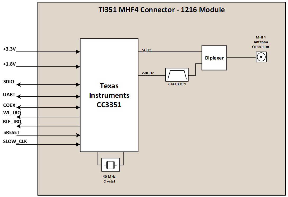
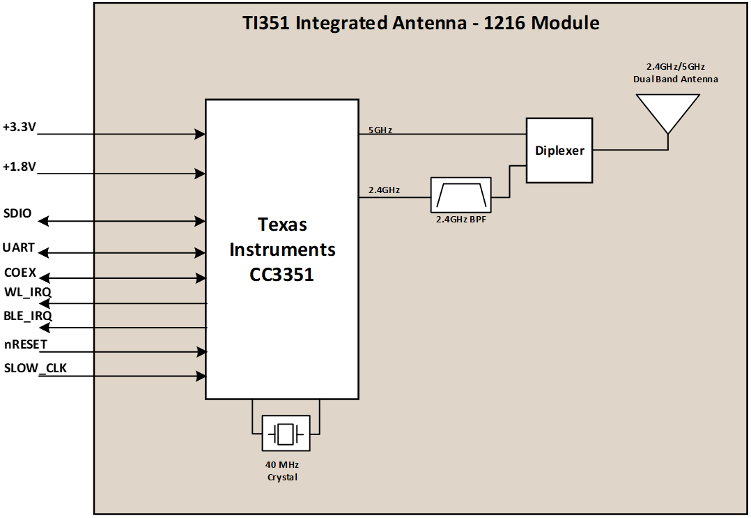
The Sona TI351 series wireless module is designed using the Texas Instruments CC3351ENJARSBR Wi-Fi 6 chipset. It is optimized for high speed, reliability, and low-power embedded applications. It is integrated with dual-band WLAN (2.4/5 GHz) and Bluetooth 5.4 (Low Energy).
| Feature | Description | ||||||||||||||||||||||||||||||||||||||||||||||||||||||||||||||||||||||||||||||||||||||||||||||||||||||||||||||||||||||||||||||||||||||||||||||||||||||||||||
|---|---|---|---|---|---|---|---|---|---|---|---|---|---|---|---|---|---|---|---|---|---|---|---|---|---|---|---|---|---|---|---|---|---|---|---|---|---|---|---|---|---|---|---|---|---|---|---|---|---|---|---|---|---|---|---|---|---|---|---|---|---|---|---|---|---|---|---|---|---|---|---|---|---|---|---|---|---|---|---|---|---|---|---|---|---|---|---|---|---|---|---|---|---|---|---|---|---|---|---|---|---|---|---|---|---|---|---|---|---|---|---|---|---|---|---|---|---|---|---|---|---|---|---|---|---|---|---|---|---|---|---|---|---|---|---|---|---|---|---|---|---|---|---|---|---|---|---|---|---|---|---|---|---|---|---|---|---|
| WLAN Features |
| ||||||||||||||||||||||||||||||||||||||||||||||||||||||||||||||||||||||||||||||||||||||||||||||||||||||||||||||||||||||||||||||||||||||||||||||||||||||||||||
| WLAN Security |
| ||||||||||||||||||||||||||||||||||||||||||||||||||||||||||||||||||||||||||||||||||||||||||||||||||||||||||||||||||||||||||||||||||||||||||||||||||||||||||||
| WLAN Channel | Channel frequencies supported.
| ||||||||||||||||||||||||||||||||||||||||||||||||||||||||||||||||||||||||||||||||||||||||||||||||||||||||||||||||||||||||||||||||||||||||||||||||||||||||||||
Bluetooth Functional Description
The Sona TI351 series wireless module includes a fully integrated Bluetooth baseband/radio. Several features and functions are listed below.
| Feature | Description |
|---|---|
| Bluetooth Interface | High-Speed UART interface |
| Bluetooth Core functionality | Supports Bluetooth LE PHYs
Legacy and Extended Advertisements Legacy and Extended Scan GATT Read/Write Secured Connection |
| Bluetooth Features | Supports features of Bluetooth Core Specification version 5.4 (Low Energy) Supported BLE Roles:
BLE Multirole enables simultaneous operation of 2 BLE roles. Up to 16 BLE connections. Standard Bluetooth test modes Transmit Power Control |
Coexistence Feature
Three coexistence lines are available to provide a means to organize wireless packet traffic for communication protocols operating in the same frequency band. When implemented, the Sona TI351 behaves as the COEX primary device to communicate to a COEX secondary device using a three-wire Packet Traffic Arbitration (PTA) interface. The coexistence signals on the TI351 are:
- COEX_GRANT: An output signal, controlled by the TI351 indicating the response of the PTA decision.
- COEX_PRIORITY: An input signal, controlled by the secondary device indicating the priority of a request signal.
- COEX_REQ: An input signal, controlled by the secondary device indicating a request to use the shared frequency band.
Power-Up Sequence
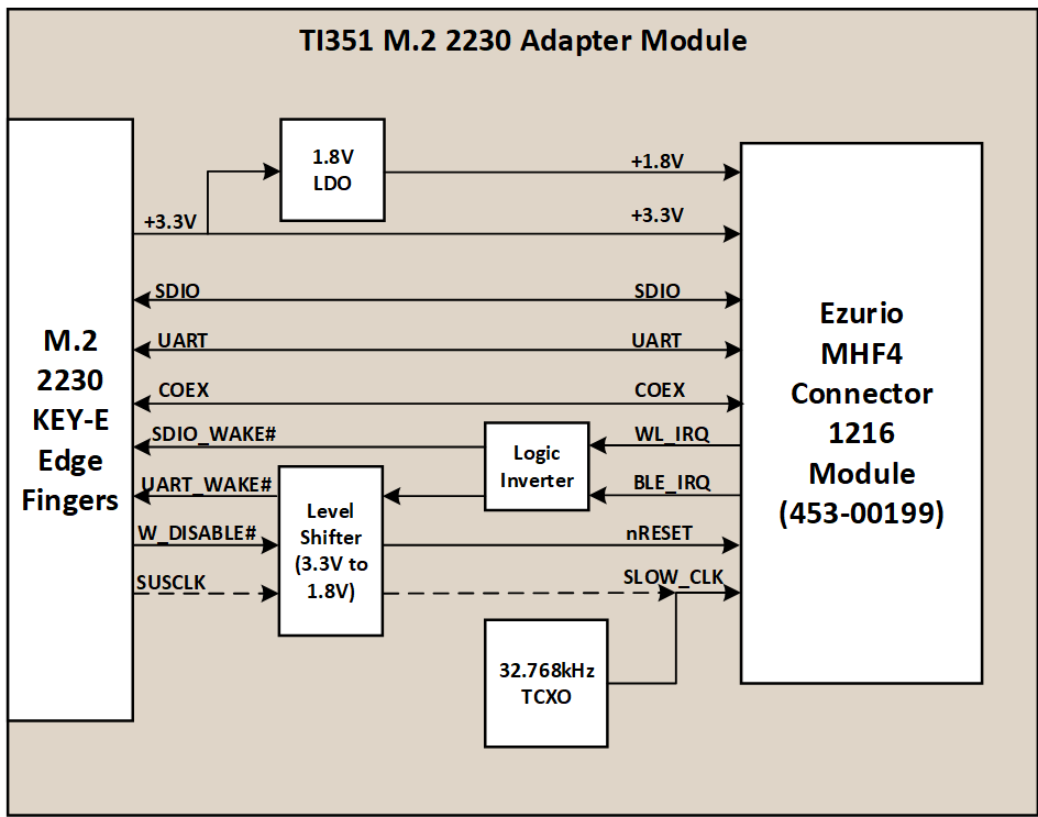
For proper operation of the Sona TI351, meet the following power-up sequence requirements.
M.2 1216 modules (453-00199 and 453-00200)
- Both module supply inputs (3.3V and VIO_1.8V) must be available and stabilized before W_DISABLE1#/nRESET line is released.
- If using an external slow clock, ensure that the clock operation is stable before W_DISABLE1#/nRESET is released (set high).
- The W_DISABLE1#/nRESET line is held low for at least 10µs after inputs are stabilized.
- The SDIO_WAKE#/HOST_IRQ_WL line on the M.2 1216 module is sensed by the module on power up. The pin is pulled low internally and must remain low when the device powers up. When this pin is connected to a host device, ensure that the line stays at a logic low level during module power-up and is not pulled high or driven high by the host platform. Some host implementations may require a buffer device to be placed between the SDIO_WAKE#/HOST_IRQ_WL module pin and the MCU GPIO pin used depending on how the MCU configures the GPIO on power up.
M.2 2230 module (453-00209)
- The module 3.3V supply input must be stable and allow at least 1ms for the module 1.8V power supply, slow clock, and level shifters to stabilize before W_DISABLE1# line is released.
- The W_DISABLE1# line is held low for at least 10µs after inputs are stabilized.
Hardware Architecture
Block Diagrams
M.2 1216 Solder-Down LGA w/MHF4 connector
M.2 1216 Solder-Down LGA w/Chip Antenna
M.2 2230 Key-E card
Pin-Out / Package Layout
Sona TI351 1216 MHF4 module Pin Assignments
| Pin # | Name | Type | Voltage Ref | Function | Comment |
|---|---|---|---|---|---|
| 1 - 3 | - | - | - | UNUSED | NC |
| 4 | 3.3V | PWR | 3.3V | DC Supply for RF Power Amplifier. | - |
| 5 | 3.3V | PWR | 3.3V | DC Supply for RF Power Amplifier. | - |
| 6 | GND | - | - | Ground | GND |
| 7 - 10 | - | - | - | UNUSED | NC |
| 11 | COEX1_RXD/COEX_REQ | I | 1.8V | External Coexistence Interface | NC if Unused |
| 12 | COEX2_TXD/COEX_GRANT | O | 1.8V | External Coexistence Interface | NC if Unused |
| 13 | COEX3/COEX_PRIORITY | I | 1.8V | External Coexistence Interface | NC if Unused |
| 14 - 16 | - | - | - | UNUSED | NC |
| 17 | GND | - | - | Ground | GND |
| 18 – 19 | - | - | - | UNUSED | NC |
| 20 | GND | - | - | Ground | GND |
| 21 – 22 | - | - | - | UNUSED | NC |
| 23 | GND | - | - | Ground | GND |
| 24 – 25 | - | - | - | UNUSED | NC |
| 26 | GND | - | - | Ground | GND |
| 27 | SUSCLK/SLOW_CLK_IN | I | 1.8V | External sleep clock (32.768kHz) | NC if Unused |
| 28 | W_DISABLE1#/nRESET | I | 1.8V | Reset line for enabling/disabling device (active low) | Hold low for >10µs after power inputs stabilized |
| 29 – 31 | - | - | - | UNUSED | NC |
| 32 | GND | - | - | Ground | GND |
| 33 – 34 | - | - | - | UNUSED | NC |
| 35 | GND | - | - | Ground | GND |
| 36 – 37 | - | - | - | UNUSED | NC |
| 38 | GND | - | - | Ground | GND |
| 39 – 40 | - | - | - | UNUSED | NC |
| 41 | GND | - | - | Ground | GND |
| 42 – 45 | - | - | - | UNUSED | NC |
| 46 | SDIO_WAKE#/HOST_IRQ_WL Important Design Note[1] | O | 1.8V | Host Wake signal Required for Wake on Wireless | Active High Interrupt[2] |
| 47 | SDIO_DATA3 | I/O | 1.8V | SDIO Data Line 3 | |
| 48 | SDIO_DATA2 | I/O | 1.8V | SDIO Data Line 2 | |
| 49 | SDIO_DATA1 | I/O | 1.8V | SDIO Data Line 1 | |
| 50 | SDIO_DATA0 | I/O | 1.8V | SDIO Data Line 0 | |
| 51 | SDIO_CMD | I/O | 1.8V | SDIO Command Line | |
| 52 | SDIO_CLK | I | 1.8V | SDIO Clock Input | |
| 53 | UART_WAKE#/HOST_IRQ_BLE | O | 1.8V | Host Wake signal (Shared SDIO mode) | Active High Interrupt[2] |
| 54 | UART_CTS | I | 1.8V | BLE HCI UART clear to send | |
| 55 | UART_TXD | O | 1.8V | BLE HCI UART serial output | |
| 56 | UART_RXD | I | 1.8V | BLE HCI UART serial input | |
| 57 | UART_RTS | O | 1.8V | BLE HCI UART request to send | |
| 58 – 61 | - | - | - | UNUSED | NC |
| 62 | GND | - | - | Ground | GND |
| 63 – 65 | - | - | - | UNUSED | NC |
| 66 | VIO_1.8V | PWR | 1.8V | DC Supply for module I/O and main | - |
| 67 | - | - | - | UNUSED | NC |
| 68 | GND | - | - | Ground | GND |
| 69 – 70 | - | - | - | UNUSED | NC |
| 71 | GND | - | - | Ground | GND |
| 72 | 3.3V | PWR | 3.3V | DC Supply for RF Power Amplifier. | - |
| 73 | 3.3V | PWR | 3.3V | DC Supply for RF Power Amplifier. | - |
| 74 | GND | - | - | Ground | GND |
| 75 | GND | - | - | Ground | GND |
| 76 | - | - | - | UNUSED | NC |
| 77 – 80 | GND | - | - | Ground | GND |
| 81 | - | - | - | UNUSED | NC |
| 82 – 85 | GND | - | - | Ground | GND |
| 86 | - | - | - | UNUSED | NC |
| 87 – 91 | GND | - | - | Ground | GND |
| 92 | - | - | - | UNUSED | NC |
| 93 - 96 | GND | - | - | Ground | GND |
| G1 – G12 | GND | - | - | Ground | GND |
Notes:
- The SDIO_WAKE#/HOST_IRQ_WL line on the M.2 1216 module is sensed by the module on power up. The pin is pulled low internally and must remain low when the device powers up. When this pin is connected to a host device, ensure that the line stays at a logic low level during module power-up and is not pulled high or driven high by the host platform. Some host implementations may require a buffer device to be placed between the SDIO_WAKE#/HOST_IRQ_WL module pin and the MCU GPIO pin used depending on how the MCU configures the GPIO on power up.
- Interrupts are active high and need an external inverter to conform to M.2 1216 LGA specification.
Sona TI351 1216 Chip Antenna Pin Assignments
| Pin # | Name | Type | Voltage Ref | Function | Comment |
|---|---|---|---|---|---|
| 1 - 3 | - | - | - | UNUSED | NC |
| 4 | 3.3V | PWR | 3.3V | DC Supply for RF Power Amplifier. | - |
| 5 | 3.3V | PWR | 3.3V | DC Supply for RF Power Amplifier. | - |
| 6 | GND | - | - | Ground | GND |
| 7 - 10 | - | - | - | UNUSED | NC |
| 11 | COEX1_RXD/COEX_REQ | I | 1.8V | External Coexistence Interface | NC if Unused |
| 12 | COEX2_TXD/COEX_GRANT | O | 1.8V | External Coexistence Interface | NC if Unused |
| 13 | COEX3/COEX_PRIORITY | I | 1.8V | External Coexistence Interface | NC if Unused |
| 14 - 16 | - | - | - | UNUSED | NC |
| 17 | GND | - | - | Ground | GND |
| 18 – 19 | - | - | - | UNUSED | NC |
| 20 | GND | - | - | Ground | GND |
| 21 – 22 | - | - | - | UNUSED | NC |
| 23 | GND | - | - | Ground | GND |
| 24 – 25 | - | - | - | UNUSED | NC |
| 26 | GND | - | - | Ground | GND |
| 27 | SUSCLK/SLOW_CLK_IN | I | 1.8V | External sleep clock (32.768kHz) | NC if Unused |
| 28 | W_DISABLE1#/nRESET | I | 1.8V | Reset line for enabling/disabling device (active low) | Hold low for >10µs after power inputs stabilized |
| 29 – 31 | - | - | - | UNUSED | NC |
| 32 | GND | - | - | Ground | GND |
| 33 – 34 | - | - | - | UNUSED | NC |
| 35 | GND | - | - | Ground | GND |
| 36 – 37 | - | - | - | UNUSED | NC |
| 38 | GND | - | - | Ground | GND |
| 39 – 40 | - | - | - | UNUSED | NC |
| 41 | GND | - | - | Ground | GND |
| 42 – 45 | - | - | - | UNUSED | NC |
| 46 | SDIO_WAKE#/HOST_IRQ_WL Important Design Note[1] | O | 1.8V | Host Wake signal Required for Wake on Wireless | Active High Interrupt[2] |
| 47 | SDIO_DATA3 | I/O | 1.8V | SDIO Data Line 3 | |
| 48 | SDIO_DATA2 | I/O | 1.8V | SDIO Data Line 2 | |
| 49 | SDIO_DATA1 | I/O | 1.8V | SDIO Data Line 1 | |
| 50 | SDIO_DATA0 | I/O | 1.8V | SDIO Data Line 0 | |
| 51 | SDIO_CMD | I/O | 1.8V | SDIO Command Line | |
| 52 | SDIO_CLK | I | 1.8V | SDIO Clock Input | |
| 53 | UART_WAKE#/HOST_IRQ_BLE | O | 1.8V | Host Wake signal (Shared SDIO mode) | Active High Interrupt[2]] |
| 54 | UART_CTS | I | 1.8V | BLE HCI UART clear to send | |
| 55 | UART_TXD | O | 1.8V | BLE HCI UART serial output | |
| 56 | UART_RXD | I | 1.8V | BLE HCI UART serial input | |
| 57 | UART_RTS | O | 1.8V | BLE HCI UART request to send | |
| 58 – 61 | - | - | - | UNUSED | NC |
| 62 | GND | - | - | Ground | GND |
| 63 – 65 | - | - | - | UNUSED | NC |
| 66 | VIO_1.8V | PWR | 1.8V | DC Supply for module I/O and main | - |
| 67 | - | - | - | UNUSED | NC |
| 68 | GND | - | - | Ground | GND |
| 69 – 70 | - | - | - | UNUSED | NC |
| 71 | GND | - | - | Ground | GND |
| 72 | 3.3V | PWR | 3.3V | DC Supply for RF Power Amplifier. | - |
| 73 | 3.3V | PWR | 3.3V | DC Supply for RF Power Amplifier. | - |
| 74 | GND | - | - | Ground | GND |
| 75 | GND | - | - | Ground | GND |
| 76 | - | - | - | UNUSED | NC |
| G1 – G4, G6 – G8, G10 – G12 | GND | - | - | Ground | GND |
Notes:
- The SDIO_WAKE#/HOST_IRQ_WL line on the M.2 1216 module is sensed by the module on power up. The pin is pulled low internally and must remain low when the device powers up. When this pin is connected to a host device, ensure that the line stays at a logic low level during module power-up and is not pulled high or driven high by the host platform. Some host implementations may require a buffer device to be placed between the SDIO_WAKE#/HOST_IRQ_WL module pin and the MCU GPIO pin used depending on how the MCU configures the GPIO on power up.
- Interrupts are active high and need an external inverter to conform to M.2 1216 LGA specification.
Sona TI351 M.2 2230 module Pin Assignments
| Pin# | M.2 Signal Name | Type | Voltage Ref | TI351 Function | Comment |
|---|---|---|---|---|---|
| 1 | GND | - | - | Ground | GND |
| 2 | 3.3V | PWR | 3.3V | DC supply voltage for module | Wait >1ms for module to stabilize after power application |
| 3 | USB_D+ | - | - | Unused | - |
| 4 | 3.3 V | PWR | 3.3V | DC supply voltage for module | Wait >1ms for module to stabilize after power application |
| 5 | USB_D- | - | - | Unused | - |
| 6 | LED1# | - | - | Unused | - |
| 7 | GND | - | - | Ground | GND |
| 8 | PCM_CLK | - | - | Unused | - |
| 9 | SDIO CLK | I | 1.8V | SDIO clock input | - |
| 10 | PCM_SYNC | - | - | Unused | - |
| 11 | SDIO CMD | I/O | 1.8V | SDIO command line | - |
| 12 | PCM_OUT | - | - | Unused | - |
| 13 | SDIO DATA0 | I/O | 1.8V | SDIO data line 0 | - |
| 14 | PCM_IN | - | - | Unused | - |
| 15 | SDIO DATA1 | I/O | 1.8V | SDIO data line 1 | - |
| 16 | LED2# | - | - | Unused | - |
| 17 | SDIO DATA2 | I/O | 1.8V | SDIO data line 2 | - |
| 18 | VIO_CFG | O | - | Sideband IO voltage indication. Connected to ground for 3.3V on the sideband IO signals. Otherwise, it must be left unconnected. | GND |
| 19 | SDIO DATA3 | I/O | 1.8V | SDIO data line 3 | - |
| 20 | UART WAKE# | O | 3.3V | BT_WAKE_OUT - Output signal to wake Host. | - |
| 21 | SDIO WAKE# | O | 1.8V | WL_HOST_WAKE - Output signal to wake host. | - |
| 22 | UART_TXD | O | 1.8V | Serial data output for the HCI UART interface. | - |
| 23 | SDIO RESET# | - | - | Unused | - |
| 32 | UART_RXD | I | 1.8V | Serial data input for the HCI UART interface. | - |
| 33 | GND | - | - | Ground | GND |
| 34 | UART_RTS | O | 1.8V | Active-Low request-to-send signal for the HCI UART interface. | - |
| 35 | PERp0 | - | - | Unused | - |
| 36 | UART_CTS | I | 1.8V | Active-Low clear-to-send signal for the HCI UART interface. | - |
| 37 | PERn0 | - | - | Unused | - |
| 38 | VENDOR DEFINED38 | - | - | Unused | - |
| 39 | GND | - | - | Ground | GND |
| 40 | VENDOR DEFINED40 | - | - | Unused | - |
| 41 | PETp0 | - | - | Unused | - |
| 42 | VENDOR DEFINED42 | - | - | Unused | - |
| 43 | PETn0 | - | - | Unused | - |
| 44 | COEX3 | I | 1.8V | COEX_PRIORITY | Unused |
| 45 | GND | - | - | Ground | GND |
| 46 | COEX_TXD | O | 1.8V | COEX_GRANT | Unused |
| 47 | REFCLKp0 | - | - | Unused | - |
| 48 | COEX_RXD | I | 1.8V | COEX_REQ | Unused |
| 49 | REFCLKn0 | - | - | Unused | - |
| 50 | SUSCLK | I | 3.3V | External Sleep Clock input (32.768KHz) | TI351 M.2 2230 card contains TCXO |
| 51 | GND | - | - | Ground | GND |
| 52 | PERST0# | - | - | Unused | - |
| 53 | CLKREQ0# | - | - | Unused | - |
| 54 | W_DISABLE2# | - | - | Unused | - |
| 55 | PEWAKE0# | - | - | Unused | - |
| 56 | W_DISABLE1# | I | 3.3V | Reset line for enabling/disabling device (active low) | Hold low for >10us after power input stabilized |
| 57 | GND | - | - | Ground | GND |
| 58 | I2C DATA | - | - | Unused | - |
| 59 | RESERVED | - | - | Unused | - |
| 60 | I2C CLK | - | - | Unused | - |
| 61 | RESERVED | - | - | Unused | - |
| 62 | ALERT# | - | - | Unused | - |
| 63 | GND | - | - | Ground | GND |
| 64 | RESERVED | - | - | Unused | - |
| 65 | RESERVED | - | - | Unused | - |
| 66 | UIM_SWP | - | - | Unused | - |
| 67 | RESERVED | - | - | Unused | - |
| 68 | UIM_POWER_SNK | - | - | Unused | - |
| 69 | GND | - | - | Ground | GND |
| 70 | UIM_POWER_SRC | - | - | Unused | - |
| 71 | RESERVED | - | - | Unused | - |
| 72 | 3.3V | PWR | 3.3V | DC supply voltage for module | Wait >1ms for module to stabilize after power application |
| 73 | RESERVED | - | - | Unused | - |
| 74 | 3.3V | PWR | 3.3V | DC supply voltage for module | Wait >1ms for module to stabilize after power application |
| 75 | GND | - | - | Ground | GND |
Mechanical Drawings
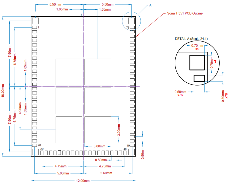
Module Footprints
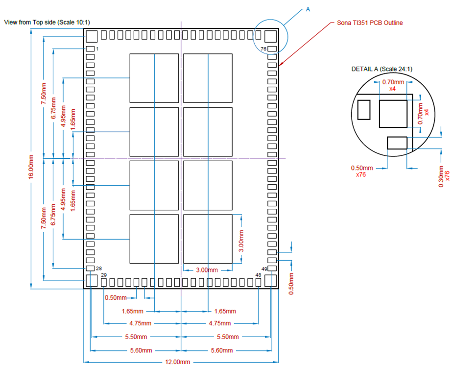
M.2 1216 MHF4 Connector (453-00199)
M.2 1216 Chip Antenna PCB Footprint (453-00200)
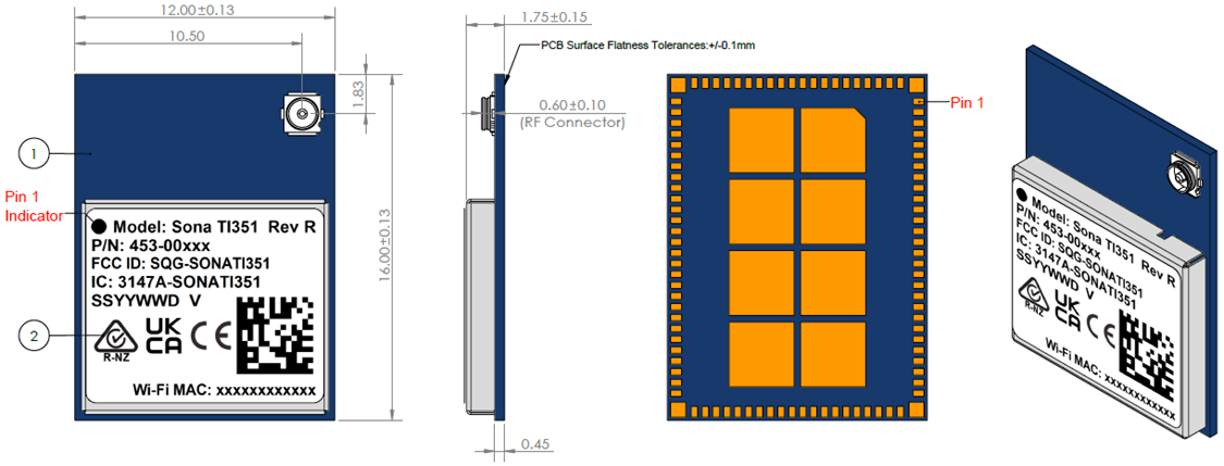
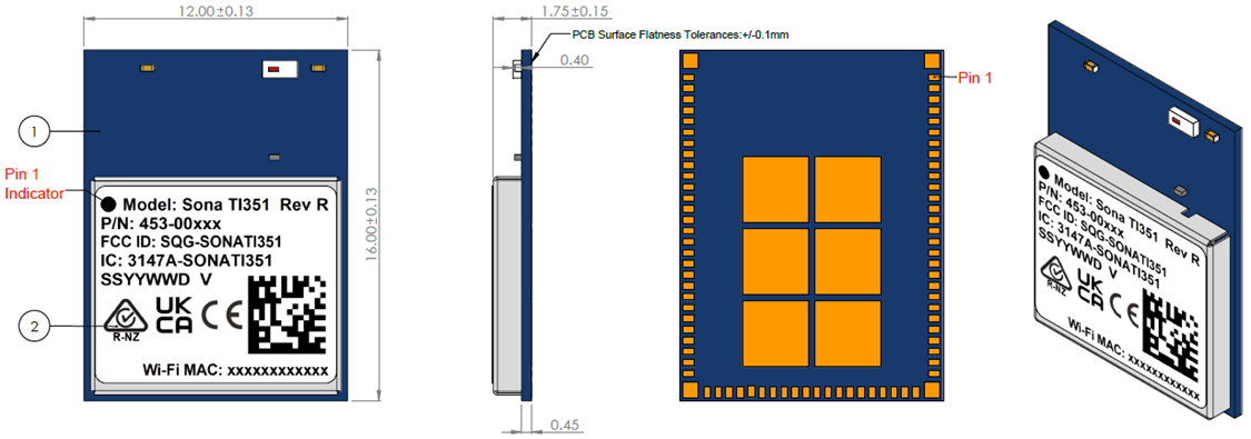
Module Dimensions
M.2 1216 Dimensions
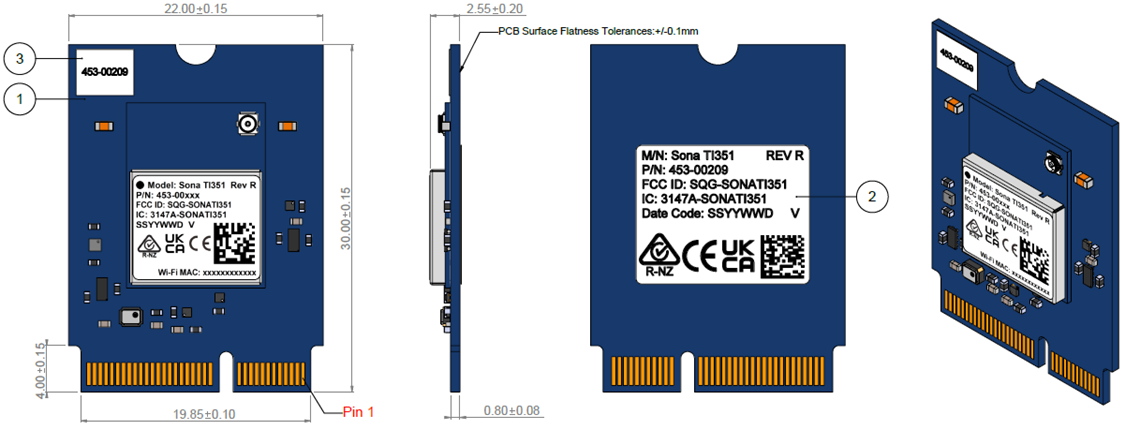
M.2 2230 Key-E (453-00209)
The dimensions of Sona TI351 M.2 2230 E-Key module are 22 x 30 x 2.55 mm.
Notes:
The Wi-Fi MAC address is located on the product label.
The last digit of Wi-Fi MAC address is assigned to either 0, 2, 4, 6, 8, A, C, E.
The BT MAC address is the Wi-Fi MAC address plus 1.
Host Interface Specifications
SDIO Specifications
The Sona TI351 module SDIO host signals are the interface for WLAN and must be 1.8V at all times as defined by the M.2 standard.
Default Mode
High Speed Mode
SDIO timing requirements
| Symbol | Parameter | Condition | Min. | Max. | Unit |
|---|---|---|---|---|---|
| fclock | Clock Frequency | Default mode High-Speed mode | - - | 26 52 | MHz |
| tHIGH | High Period | Default mode High-Speed mode | 10 7 | - - | ns |
| tLOW | Low Period | Default mode High-Speed mode | 10 7 | - - | ns |
| tTLH | Clock rise time | Default mode High-Speed mode | - - | 10 3 | ns |
| tTHL | Clock fall time | Default mode High-Speed mode | - - | 10 3 | ns |
| tISU | Setup time, input valid before CLK ↑ | Default mode High-Speed mode | 5 6 | - - | ns |
| tIH | Hold time, input valid after CLK ↑ | Default Speed High-Speed mode | 5 2 | - - | ns |
| tODLY | Delay time, CLK ↓ to output valid | Default mode High-Speed mode | 2 2 | 14 14 | ns |
| CL | Capacitive load (output lines) | Default mode High-Speed mode | 15 | 40 | pF |
| 15 | 40 | pF |
UART Interface Specifications
The Sona TI351 series 4-wire UART is the main host interface for BLE access through the host controller interface (HCI) transport layer.
When using the UART interface with a host, take care to connect the lines correctly. The signal names as listed in the Pin Assignment Tables of Pin Out / Package Layout are with respect to the TI351 module.
- UART_TXD must be connected to host side UART_RXD
- UART_RXD must be connected to host side UART_TXD
- UART_CTS must be connected to host side UART_RTS
- UART_RTS must be connected to host side UART_CTS
UART timing specifications
| Parameter | Condition | Min | Typ | Max | Unit |
|---|---|---|---|---|---|
| Baud rate | 37.5 | — | 4364 | kbps | |
| Baud rate accuracy per byte | Receive/Transmit | -2.5 | — | +1.5 | % |
| Baud rate accuracy per bit | Receive/Transmit | -12.5 | — | +12.5 | % |
| CTS low to TX_DATA on | Hardware Flow Control | 0 | 2 | — | ms |
| CTS high to TX_DATA off | — | — | 1 | Byte | |
| CTS high pulse wide | 1 | — | — | bit | |
| RTS low to RX_DATA on | 0 | 2 | — | ms | |
| RTS high to RX_DATA off | Interrupt set to ¼ FIFO | — | — | 16 | Byte |
Electrical Characteristics
Absolute Maximum Ratings
Absolute maximum ratings are those values beyond which damage to the device can occur. Functional operation under these conditions, or at any other condition beyond those indicated in the operational sections of this document, is not recommended.
Note: Maximum rating for signals follows the supply domain of the signals.
| Symbol (Domain) | Description | Max Rating | Unit |
|---|---|---|---|
| 3.3V VPA | VDD PA power supply (M.2 1216) | 4.2 | V |
| VIO_1.8V | DC supply voltage for digital I/O (M.2 1216) | 2.1 | V |
| 3.3V | External 3.3V power supply (M.2 2230 E-Key) | 3.6 | V |
| Storage | Storage temperature | -55 to +125 | °C |
| ESD | Electrostatic discharge tolerance | 2000 | V |
Recommended Operating Conditions
| Symbol (Domain) | Parameter | Min | Typ | Max | Unit |
|---|---|---|---|---|---|
| 3.3V VPA | VDD PA power supply (M.2 1216) | 3.0 | 3.3 | 3.6 | V |
| VIO_1.8V | DC supply voltage for digital I/O (M.2 1216) | 1.62 | 1.8 | 1.98 | V |
| 3.3V | External 3.3V power supply (M.2 2230 E-Key) | 3.0 | 3.3 | 3.6 | V |
| T-ambient | Ambient temperature | -40 | 25 | +85 | °C |
DC Electrical Characteristics / Current Consumption
The following table lists the general DC electrical characteristics over recommended operating conditions (unless otherwise specified).
General DC electrical characteristics (For 1.8V operation VDDIO)
| Symbol | Parameter | Conditions | Min | Typ | Max | Unit |
|---|---|---|---|---|---|---|
| VIH | High Level Input Voltage | — | 0.65 x VDDIO | — | VDDIO | V |
| VIL | Low Level Input Voltage | — | 0 | — | 0.35 x VDDIO | V |
| VOH | Output high Voltage | 4mA | VDDIO – 0.45 | — | VIO | V |
| VOL | Output low Voltage | 4mA | 0 | — | 0.45 | V |
The following table lists the nominal device current consumption at room temperature.
Low power current consumption
| Mode | Conditions | Model variant | Supply | Typ | Unit |
|---|---|---|---|---|---|
| Shutdown | External supplies available Device in reset (nRESET low) | M.2 1216 | VIO_1.8V | 10 | µA |
| 3.3V VPA | 2 | µA | |||
| M.2 2230 | 3.3V | TBD | µA | ||
| Sleep | Low Power Mode RAM retention | M.2 1216 | VIO_1.8V | 330 | µA |
| 3.3V VPA | 2 | µA | |||
| M.2 2230 | 3.3V | TBD | µA |
Radio Characteristics
WLAN Radio Receiver Characteristics
The following tables summarize the Sona TI351 series wireless module receiver characteristics.
Typical WLAN receiver characteristics for 2.4 GHz single chain operation, room temperature
| Item | Parameter | Conditions | Min | Typ | Max | Unit | |
|---|---|---|---|---|---|---|---|
| Frequency Range | Receive input frequency range | — | 2.412 | — | 2.472 | GHz | |
| RX Sensitivity | DSSS, 1 Mbps | 8% PER | — | -97 | — | dBm | |
| CCK, 11 Mbps | 8% PER | — | -88 | — | |||
| OFDM, 6 Mbps | 10% PER | — | -92 | — | |||
| OFDM, 54 Mbps | 10% PER | — | -74 | — | |||
| HT20, MCS0 | 10% PER | — | -92 | — | |||
| HT20, MCS7 | 10% PER | — | -72 | — | |||
| HE20, MCS0 | 10% PER | — | -91 | — | |||
| HE20, MCS7 | 10% PER | — | -72 | — | |||
Maximum Input Level | DSSS, 1 Mbps | 8% PER | — | 0 | — | dBm | |
| OFDM, 6 Mbps; HT MCS0, HE MCS0 | 10% PER | — | 0 | — | |||
| OFDM, 54 Mbps; HT MCS7, HE MCS7 | 10% PER | — | -9 | — | |||
ACI – Adjacent Channel Rejection | DSSS, 1 Mbps | — | 20 | — | dB | ||
| CCK, 11 Mbps | — | 39 | — | ||||
| OFDM, 6 Mbps | — | 20 | — | ||||
| OFDM, 54 Mbps | — | 3 | — | ||||
| HT20, MCS0 | — | 20 | — | ||||
| HT20, MCS7 | — | 3 | — | ||||
| HE20, MCS0 | — | 16 | — | ||||
| HE20, MCS7 | — | -1 | — | ||||
Typical WLAN receiver characteristics for 5 GHz single chain operation, room temperature
| Item | Parameter | Conditions | Min | Typ | Max | Unit |
|---|---|---|---|---|---|---|
| Frequency Range | Receive input frequency range | — | 5.15 | — | 5.85 | GHz |
| RX Sensitivity | OFDM, 6 Mbps | 10% PER | — | -92 | — | dBm |
| OFDM, 54 Mbps | — | -74 | — | |||
| HT20, MCS0 | — | -91 | — | |||
| HT20, MCS7 | — | -72 | — | |||
| HE20, MCS0 | — | -89 | — | |||
| HE20, MCS7 | — | -70 | — |
WLAN Transmitter Characteristics
The following tables summarize the Sona TI351 series wireless module WLAN transmitter characteristics at room temperature.
WLAN transmitter characteristics for 2.4 GHz operation (VPA = 3.3V, VDDIO = 1.8V)
| Parameter | Conditions | Min | Typ | Max | Unit |
|---|---|---|---|---|---|
| Transmit output frequency range | — | 2.402 | — | 2.472 | GHz |
| Output power[1] | DSSS, 1 Mbps | — | — | 17 | dBm |
| CCK, 11 Mbps | — | — | 17 | ||
| OFDM, 6 Mbps | — | — | 16.7 | ||
| OFDM, 54 Mbps | — | — | 15.3 | ||
| HT20, MCS0 | — | — | 16.7 | ||
| HT20, MCS7 | — | — | 15.3 | ||
| HE20, MCS0 | — | — | 16.5 | ||
| HE20, MCS7 | — | — | 14.5 |
Note 1: Final TX power values on each channel are limited by regulatory requirements.
M.2 1216 module WLAN transmitter current consumption at 2.4 GHz (VPA= 3.3V, VDDIO = 1.8V) – at maximum TX power setting
| Modulation | VPA 3.3V Current Consumption (mA) | VIO 1.8V Current Consumption (mA) |
|---|---|---|
| DSSS, 1 Mbps | 245 | 90 |
| CCK, 11 Mbps | 240 | 90 |
| OFDM, 6 Mbps | 230 | 95 |
| OFDM, 54 Mbps | 195 | 95 |
| HT20, MCS0 | 225 | 95 |
| HT20, MCS7 | 200 | 95 |
| HE20, MCS0 | 225 | 95 |
| HE20, MCS7 | 200 | 95 |
M.2 2230 module WLAN transmitter current consumption at 2.4 GHz (VDD = 3.3V) – at maximum TX power setting
| Modulation | 3.3V Current Consumption (mA) |
|---|---|
| DSSS, 1 Mbps | 355 |
| CCK, 11 Mbps | 360 |
| OFDM, 6 Mbps | 350 |
| OFDM, 54 Mbps | 320 |
| HT20, MCS0 | 350 |
| HT20, MCS7 | 320 |
| HE20, MCS0 | 350 |
| HE20, MCS7 | 320 |
WLAN transmitter characteristics for 5 GHz operation (VBAT=3.3V, VDDIO=1.8V)
| Parameter | Conditions | Min | Typ | Max | Unit |
|---|---|---|---|---|---|
| Transmit output frequency range | — | 5.15 | — | 5.85 | GHz |
| Output power[2] | OFDM, 6 Mbps | — | — | 15.5 | dBm |
| OFDM, 54 Mbps | — | — | 13.0 | ||
| HT20, MCS0 | — | — | 15.0 | ||
| HT20, MCS7 | — | — | 13.0 | ||
| HE20, MCS0 | — | — | 15.0 | ||
| HE20, MCS7 | — | — | 13.0 |
Note 2: Final TX power values on each channel are limited by regulatory requirements.
M.2 1216 module WLAN transmitter current consumption at 5 GHz (VPA= 3.3V, VDDIO = 1.8V) – at maximum TX power setting
| Modulation | VPA 3.3V Current Consumption (mA) | VIO 1.8V Current Consumption (mA) |
|---|---|---|
| OFDM, 6 Mbps | 240 | 150 |
| OFDM, 54 Mbps | 180 | 150 |
| HT20, MCS0 | 240 | 150 |
| HT20, MCS7 | 180 | 150 |
| HE20, MCS0 | 235 | 150 |
| HE20, MCS7 | 180 | 150 |
M.2 2230 module WLAN transmitter current consumption at 5 GHz (VDD = 3.3V) – at maximum TX power setting
| Modulation | 3.3V Current Consumption (mA) |
|---|---|
| OFDM, 6 Mbps | 400 |
| OFDM, 54 Mbps | 335 |
| HT20, MCS0 | 400 |
| HT20, MCS7 | 340 |
| HE20, MCS0 | 400 |
| HE20, MCS7 | 340 |
Bluetooth Transmitter Characteristics
The following tables describe the performance of the Bluetooth Low Energy transmitter and receiver and the current consumption at 25°C.
BLE RF Specifications (VPA = 3.3V, VDDIO = 1.8V)
| Parameter | Conditions | Min | Typ | Max | Unit | |
|---|---|---|---|---|---|---|
| Frequency range | — | 2402 | — | 2480 | MHz | |
| Rx saturation | GFSK, PER ≤ 30.8% | — | 0 | — | dBm | |
| Rx sensitivity[1] | GFSK, PER ≤ 30.8% | 1 Mbps | — | -97[2] | — | dBm |
| 2 Mbps | — | -94[2] | — | dBm | ||
| 500 Kbps | — | -99 | — | dBm | ||
| 125 Kbps | — | -102 | — | dBm | ||
| C/I Co-channel rejection[3] | Modulated interferer | 1 Mbps | — | 10 | — | dB |
| 2 Mbps | — | 10 | — | dB | ||
| 500 Kbps | — | 10 | — | dB | ||
| 125 Kbps | — | 10 | — | dB | ||
| C/I 1 MHz Selectivity[3] | Modulated interferer at ±1MHz | 1 Mbps | — | 0/0 | — | dB |
| 500 Kbps | — | 0/0 | — | dB | ||
| 125 Kbps | — | 0/0 | — | dB | ||
| C/I 2 MHz Selectivity[3] | Modulated interferer at ±2MHz | 1 Mbps | — | -35/-28 | — | dB |
| 2 Mbps | — | 0/0 | — | dB | ||
| 500 Kbps | — | -35/-25 | — | dB | ||
| 125 Kbps | — | -37/-30 | — | dB | ||
| C/I 3 MHz Selectivity[3] | Modulated interferer at ±3MHz | 1 Mbps | — | -38/-32 | — | dB |
| 500 Kbps | — | -40/-37 | — | dB | ||
| 125 Kbps | — | -39/-36 | — | dB | ||
| C/I 4 MHz Selectivity[3] | Modulated interferer at ±4MHz | 1 Mbps | — | -45/-40 | — | dB |
| 2 Mbps | — | -35/-28 | — | dB | ||
| 500 Kbps | — | -45/-40 | — | dB | ||
| 125 Kbps | — | -45/-41 | — | dB | ||
| Out-of-Band Blocking Performance | 1 Mbps Wanted signal @ -67 dBm | 30-2000 MHz | — | -23 | — | dBm |
| 2-2.399 GHz | — | -30 | — | dBm | ||
| 2.484-3 GHz | — | -30 | — | dBm | ||
| 3-6 GHz | — | -21 | — | dBm | ||
| Intermodulation | Wanted signal at 2402MHz, -64 dBm Interferers at 2405 and 2408 MHz | 1 Mbps | — | -40 | — | dBm |
| 2 Mbps | — | -44 | — | dBm | ||
| Tx power[4] | — | — | — | 7 | dBm | |
Notes:
- Dirty Tx is Off.
- BLE 1M PHY sensitivity on channels 17 and 39 may degrade by up to 2.5dB, BLE 2M PHY sensitivity on channel 17 may degrade by up to 1.5 dB
- Wanted signal levels differ with PHY: 1 Mbps @ -67dBm, 2 Mbps @ -67 dBm, 500 kbps @ -72 dBm, 125 kbps @-79 dBm.
- The Bluetooth LE TX power cannot exceed 10 dBm EIRP specification limit. The antenna gain/loss must be factored in so as not to exceed the limit.
M.2 1216 modules BLE radio current consumption (VPA = 3.3V, VDDIO = 1.8V)
| Operation Mode | VPA Current Consumption (mA) | VDD_IO Current Consumption (mA) |
|---|---|---|
| BLE TX[1] | 110 | 90 |
| BLE RX | 0 | 60 |
Notes:
- BLE TX power setting = 10 dBm
M.2 2230 module BLE radio current consumption (VDD = 3.3V)
| Operation Mode | VDD Current Consumption (mA) |
|---|---|
| BLE TX[1] | 200 |
| BLE RX | 60 |
Notes:
- BLE TX power setting = 10 dBm
Slow Clock Oscillator Requirements
The Sona TI351 modules use a slow clock running at 32.768 kHz for low power modes. On the M.2 1216 modules the slow clock can be generated internally or supplied externally. The internal oscillator is less accurate and consumes more power than sourcing the slow clock externally. When using the internal slow clock oscillator, leave the SUSCLK/SLOW_CLK_IN pin (Pin 27) unconnected.
An external clock source must meet the requirements listed in Table 24. This clock should be fed to the SUSCLK/SLOW_CLK_IN pin (Pin 27). The clock operation needs to be stable before the W_DISABLE1#/nRESET line is de-asserted to enable the device.
External Slow Clock Requirements (453-00199 and 453-00200 modules)
| Parameter | Conditions | Min | Typ | Max | Unit |
|---|---|---|---|---|---|
| Clock Frequency | Square wave | — | 32768 | — | Hz |
| Frequency accuracy | Initial + temperature + aging | — | — | ±250 | ppm |
| Input Duty Cycle | OFDM, 54 Mbps | 30 | 50 | 70 | % |
| Rise and Fall times | 10/90% and 90/10% | — | — | 100 | ns |
| Input Low Level | 0 | — | 0.35 x VIO_1.8 | V | |
| Input High Level | 0.65 x VIO_1.8 | — | 1.95 | V | |
| Input Impedance | 1 | — | — | MΩ | |
| Input Capacitance | — | — | 5 | pF |
Note: The M.2 2230 module (453-00209) includes an on module external slow clock oscillator.
Integration Guidelines
The following is a list of RF layout design guidelines and recommendations when installing an Ezurio radio into your device.
- Do not run any antenna cables directly above or directly below the radio.
- Do not place any parts or run any high-speed digital lines below the radio.
- Ensure that there is the maximum allowable spacing separating the antenna connectors on the Ezurio radio from the antenna. In addition, do not place antennas directly above or directly below the radio.
- Ezurio recommends the use of a double-shielded cable for the connection between the radio and the antenna elements.
- Be sure to put a 10uF/16V/0603 capacitor on EACH 3.3V power pin. Also, place that capacitor as close as possible to the pin to make sure the internal PMU is working correctly.
- Use proper electro-static-discharge (ESD) procedures when installing the Ezurio radio module. To avoid negatively impacting Tx power and receiver sensitivity, do not cover the antennas with metallic objects or components.
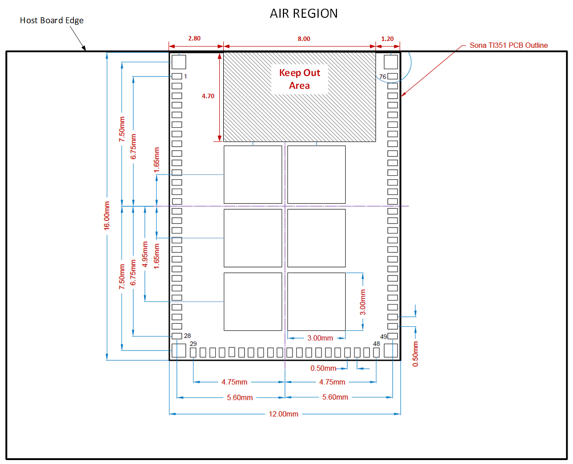
Sona TI351 Integrated Antenna Guidelines
The Sona TI351 integrated antenna variant (453-00200) has specific placement and layout design guidelines that must be followed.
- The Sona TI351 Integrated antenna variant MUST BE located at the edge of the Host PCB and surrounded by ground on three sides.
- The antenna keep out region as defined in Figure 14 must be kept clear of copper on all layers of the host PCB.
- Extending the ground on the Host PCB ≥ 15mm from the module edge in each direction will optimize antenna performance.
Antenna Keep-Out on Host PCB
Surface Mount Conditions
The following soldering conditions are recommended to ensure device quality.
Soldering
Note: When soldering, the stencil thickness should be ≥ 0.1 mm.
Convection reflow or IR/Convection reflow (one-time soldering or two-time soldering in air or nitrogen environment)
Measuring point – IC package surface
Temperature profile:
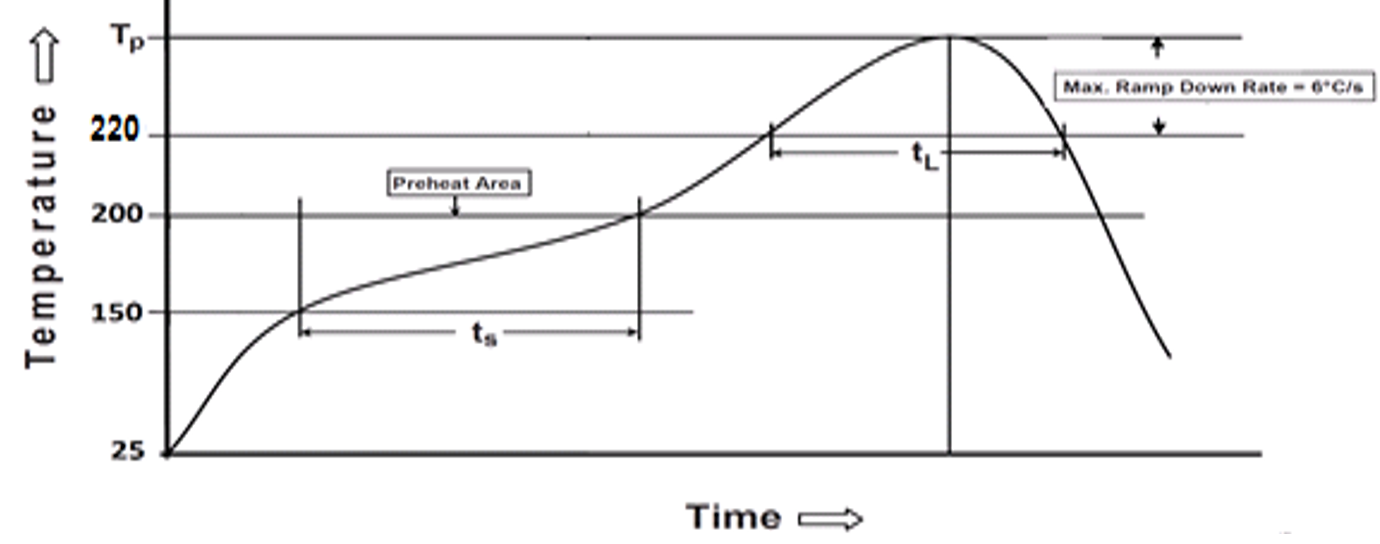
- Solder paste alloy: SAC305(Sn96.5 / Ag3.0 / Cu 0.5)
- Pre-heat temperature: 150℃ ~ 200℃; Soak time: 60 second ~ 120 second
- Peak temperature: 235℃ ~ 250℃
- Time above 220℃: 40 second ~ 90 second
- Optimal cooling rate < 3℃/second
- The oxygen concentration < 2000 ppm
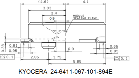
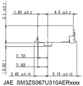
M.2 2230 Key-E Mounting
The Sona TI351 M.2 2230 module connects to the host via a standard PCI EXPRESS M2 connector. The Kyocera (www.Kyocera-connector.com) 6411 series provides 1.8 mm, 2.3 mm and 3.2 mm connector heights and the JAE (https://www.jae.com/en/ ) SM3 series provides 1.2 mm, 2.15 mm, 3.1 mm and 4.1 mm connector heights.
Because the Sona TI351 M.2 2230 module is a single-side component module, we recommend the following part numbers which have 2.3 mm and 3.1 mm connector height:
| M.2 Key-E Connector | Connector Height |
|---|---|
| KYOCERA 24-6411-067-101-894E | 2.3 mm |
| JAE SM3ZS067U310AERxxxx | 3.1 mm |
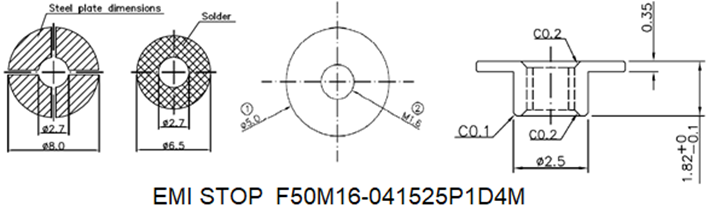
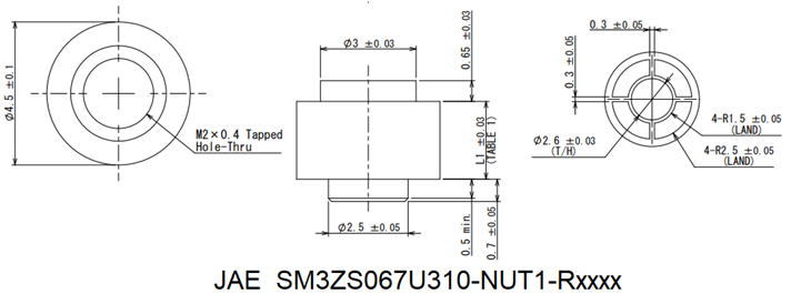
The stand-off mating to the recommend 2.3 mm connector from EMI STOP (www.EMISTOP.com) is part number F50M16-041525P1D4M and 3.1mm from JAE (https://www.jae.com/en/ ) is part number SM3ZS067U310-NUT1-Rxxxx.
| M.2 Key-E Connector | Stand-off |
|---|---|
| KYOCERA 24-6411-067-101-894E | EMI STOP F50M16-041525P1D4M |
| JAE SM3ZS067U310AERxxxx | JAE SM3ZS067U310-NUT1-Rxxxx |
Detailed layout and stencil opening are shown as follows.
Application Note for Surface Mount Modules
Introduction
Ezurio’s surface mount modules are designed to conform to all major manufacturing guidelines. This application note is intended to provide additional guidance beyond the information that is presented in the user manual. This application note is considered a living document and will be updated as new information is presented.
The modules are designed to meet the needs of several commercial and industrial applications. They are easy to manufacture and conform to current automated manufacturing processes.
Shipping and Labeling
M.2 1216 Solder-Down
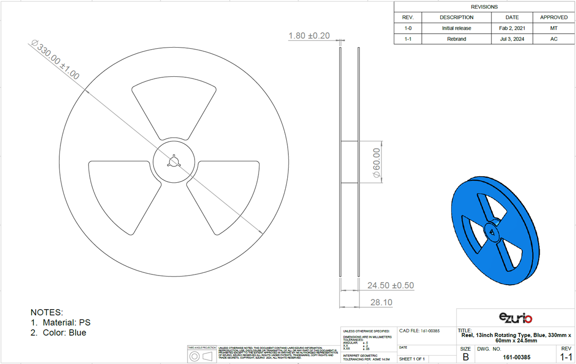
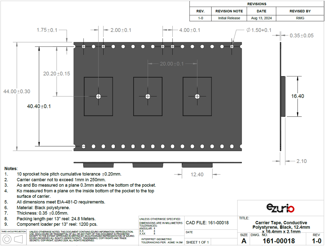
There are 1000 Sona TI351 modules taped in a reel (and packaged in a pizza box) and five boxes per carton (5,000 modules per carton). Reel, boxes, and carton are labeled with the appropriate labels.
The following labels are located on the antistatic bag.
The following label is placed on the reel, bag and pizza box.
The following package label is located on adjacent sides of the master carton.
M.2 2230 Key-E Card
The following label is placed on the bag and the inner box.

The following label is located on the adjacent sides of the master carton.
Reflow Parameters
Cautions when Removing the SIP from the Platform for RMA
- Bake the platform before removing the Sona TI351 module from the platform. Reference baking conditions.
- Remove the Sona TI351 module by using a hot air gun. This process should be carried out by a skilled technician.
Recommended conditions:
One-side component platform:
- Set the hot plate at 280°C.
- Put the platform on the hot plate for 8~10 seconds.
Remove the device from platform.
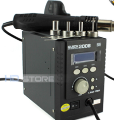
Two-side components platform:
- Use two hot air guns.
- On the bottom, use a pre-heated nozzle (temp setting of 200~250°C) at a suitable distance from the platform PCB.
On the top, apply a remove nozzle (temp setting of 330°C). Heat until device can be removed from platform PCB.
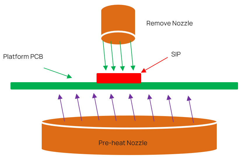
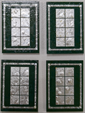
- Remove the residue solder under the bottom side of device. (Note: Alternate module pictured as an example)
| Not Accepted for RMA | Accepted for RMA Analysis |
|---|---|
 |  |
- Remove and clean the residue flux as needed.
Precautions for Use
- Opening/handling/removing must be done on an anti-ESD treated workbench. All workers must also have undergone anti-ESD treatment.
- The devices should be mounted within one year of the date of delivery.
- The Sona TI351 1216 modules are MSL level 4 rated.
Environmental and Reliability
Environmental Requirements
Required Storage Conditions
Prior to Opening the Dry Packing
The following are required storage conditions prior to opening the dry packing:
- Normal temperature: 5~40˚C
- Normal humidity: 80% (Relative humidity) or less
- Storage period: One year or less
Note: Humidity means relative humidity.
After Opening the Dry Packing
The following are required storage conditions after opening the dry packing (to prevent moisture absorption):
Storage conditions for one-time soldering:
- Temperature: 5-25°C
- Humidity: 60% or less
- Period: 72 hours or less after opening
Storage conditions for two-time soldering
Storage conditions following opening and prior to performing the 1st reflow:
- Temperature: 5-25°C
- Humidity: 60% or less
- Period: A hours or less after opening
Storage conditions following completion of the 1st reflow and prior to performing the 2nd reflow
- Temperature: 5-25°C
- Humidity: 60% or less
- Period: B hours or less after completion of the 1st reflow
Note: Should keep A+B within 72 hours.
Temporary Storage Requirements after Opening
The following are temporary storage requirements after opening:
- Only re-store the devices once prior to soldering.
- Use a dry box or place desiccant (with a blue humidity indicator) with the devices and perform dry packing again using vacuumed heat-sealing.
The following indicate the required storage period, temperature, and humidity for this temporary storage:
Storage temperature and humidity:
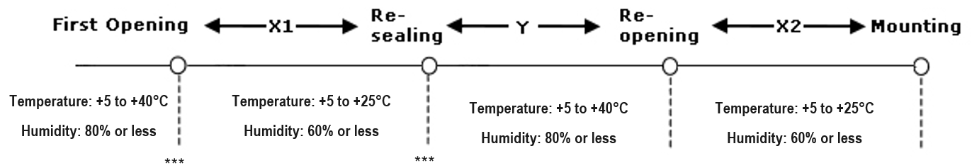
*** - External atmosphere temperature and humidity of the dry packing
Storage period:
- X1+X2 – Refer to After Opening the Dry Packing storage requirements. Keep is X1+X2 within 72 hours.
- Y – Keep within two weeks or less.
Baking Conditions
Baking conditions and processes for the module follow the J-STD-033 standard which includes the following:
- The calculated shelf life in a sealed bag is 12 months at <40℃ and <80% relative humidity.
- Once the packaging is opened, the SiP must be mounted (per MSL4/Moisture Sensitivity Level 4) within 72 hours at <30˚C and <60% relative humidity.
If the SiP is not mounted within 72 hours or if, when the dry pack is opened, the humidity indicator card displays >10% humidity, then the product must be baked for 48 hours at 125 ˚C (±5 ˚C).
Reliability Tests
The Sona TI351 modules were tested for reliability. Test items and the corresponding standards are shown in the following sections.
Environmental and Mechanical
The following are the reliability test procedures and results.
Sona TI351 M.2 1216 Solder-down Module Reliability Test Items and Standards
| Test Item | Specification | Standard | Test Result |
|---|---|---|---|
| Thermal Shock |
| *JESD22-A106 *IEC 60068-2-14 for dwell time and number of cycles | PASS |
| Vibration Non-operating Unpackaged device |
| JEDEC 22-B103B (2016) | PASS |
| Mechanical Shock Non-operating Unpackaged device |
| JEDEC 22-B110B.01 (2019) | PASS |
Sona TI351 M.2 2230 E-Key Module Reliability Test Item and Standards
| Test Item | Specification | Standard | Test Result |
|---|---|---|---|
| Thermal Shock |
| *JESD22-A106 *IEC 60068-2-14 for dwell time and number of cycles | PASS |
| Vibration Non-operating Unpackaged device |
| JEDEC 22-B103B (2016) | PASS |
| Mechanical Shock Non-operating Unpackaged device |
| JEDEC 22-B110B.01 (2019) | PASS |
Reliability Prediction
The predicted method refers to Telcordia SR-232 Issue 4 (2016)
Sona TI351 MTBF analysis
| Ezurio Part Number | Environment | Test Result 45 ℃ (Hours) |
|---|---|---|
| 453-00199R 453-00199C 453-00200R 453-00200C | Ground, Fixed, Uncontrolled Ground, Mobile | 10252962.09 5234443.907 |
| Ezurio Part Number | Environment | Test Result 85 ℃ (Hours) |
|---|---|---|
| 453-00199R 453-00199C 453-00200R 453-00200C | Ground, Fixed, Uncontrolled Ground, Mobile | 1988175.12 1014808.30 |
| Ezurio Part Number | Environment | Test Result 45 ℃ (Hours) |
|---|---|---|
| 453-00209 | Ground, Fixed, Uncontrolled Ground, Mobile | 4167380.48 2693697.55 |
| Ezurio Part Number | Environment | Test Result 85 ℃ (Hours) |
|---|---|---|
| 453-00209 | Ground, Fixed, Uncontrolled Ground, Mobile | 701816.41 463835.06 |
Regulatory, Qualification & Certifications
Regulatory Approvals
Note: For complete regulatory information, refer to the Sona TI351 Regulatory Information document which is also available from the Sona TI351 product page.
The Sona TI351 holds current certifications in the following countries (pending):
Sona TI351 Regulatory Certifications
| Country/Region | Regulatory ID |
|---|---|
| USA (FCC) | SQG-SONATI351 |
| EU | N/A |
| UKCA | N/A |
| Canada (ISED) | 3147A-SONATI351 |
| Japan (MIC) | pending |
| Australia | N/A |
| New Zealand | N/A |
| Korea | pending |
Certified Antennas
The Sona TI351 MHF4 (453-00199) module was tested with the antennas listed in the following table.
Sona TI351 MHF4 external certified antenna list
| Manufacturer | Model | Ezurio Part Number | Type | Connector | Peak Gain (dBi) @ 2.4 GHz | Peak Gain (dBi) @ 5 GHz |
|---|---|---|---|---|---|---|
| Ezurio (Laird Connectivity) | FlexPIFA | 001-0021 | PIFA | MHF4L | 2.5 | 3.0 |
| Ezurio (Laird Connectivity) | FlexPIFA | EFB2455A3S-15MH4L | PIFA | MHF4L | 2.5 | 3.0 |
| Ezurio (Laird Connectivity) | FlexPIFA 6E | EFB2471A3S-10MH4L | PIFA | MHF4L | 2.2 | 3.9 |
| Ezurio (Laird Connectivity) | Mini NanoBlade Flex | EMF2449A1-10MH4L | PCB Dipole | MHF4L | 2.8 | 3.4 |
| Ezurio (Laird Connectivity) | Mini NanoBlade Flex 6E | EMF2471A3S-10MH4L | PCB Dipole | MHF4L | 2.4 | 4.4 |
| Ezurio (Laird Connectivity) | NanoBlade | ENB2449A1-10MH4L | PCB Dipole | MHF4L | 3.19 | 4.1 |
| Joymax Electronics | Dipole | TWX-100BRSAX-2001 / TWX-100BRS3B | Dipole | RP-SMA | 2 | 4.0 |
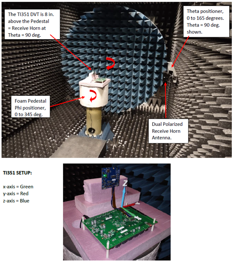
Sona TI351 (453-00200) Chip Antenna Performance Characteristics
The TI351 Chip antenna module radiated performance depends on the host PCB layout. The TI351 development board (453-00200-K1) was used for the chip antenna tuning and 453-00200 antenna performance evaluation. To obtain similar performance, follow the guidelines presented in Section 14 RF Layout Guidelines for the chip antenna host PCB layout.
Sona TI351 Chip Antenna Radiated Performance
| Frequency (MHz) | TRP (dBm) | Total Gain (dBi) |
|---|---|---|
| 2412 | -6.02 | 0.93 |
| 2442 | -5.43 | 1.96 |
| 2472 | -5.71 | 1.99 |
| 5180 | -5.31 | -0.11 |
| 5500 | -3.19 | 1.79 |
| 5825 | -3.16 | 1.91 |
Notes:
The set Antenna Power = 0 dBm
The Total Gain is calculated assuming the Antenna Power = 0 dBm
Test Setup
2442 MHz Radiated Performance
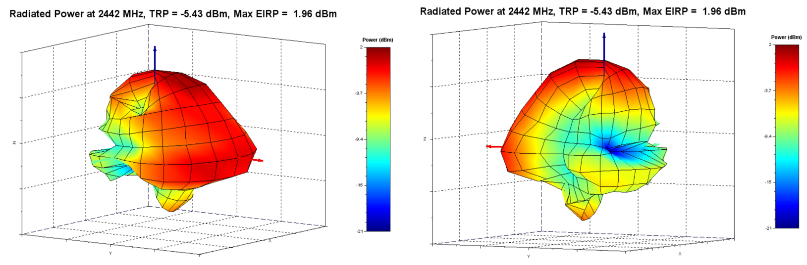
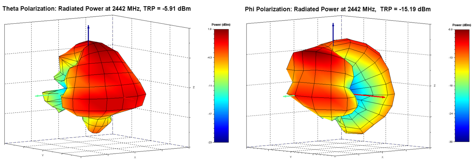
The patterns at other frequencies in the 2.4 GHz band exhibit the same radiated performance characteristics.
5500 MHz Radiated Performance
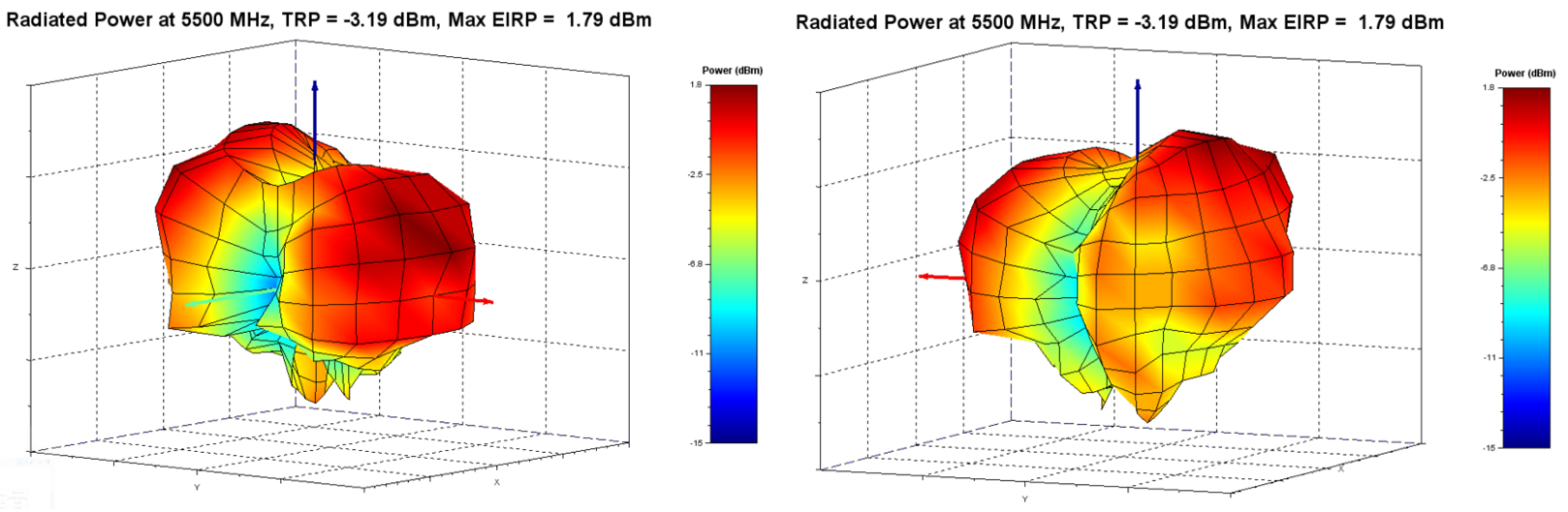
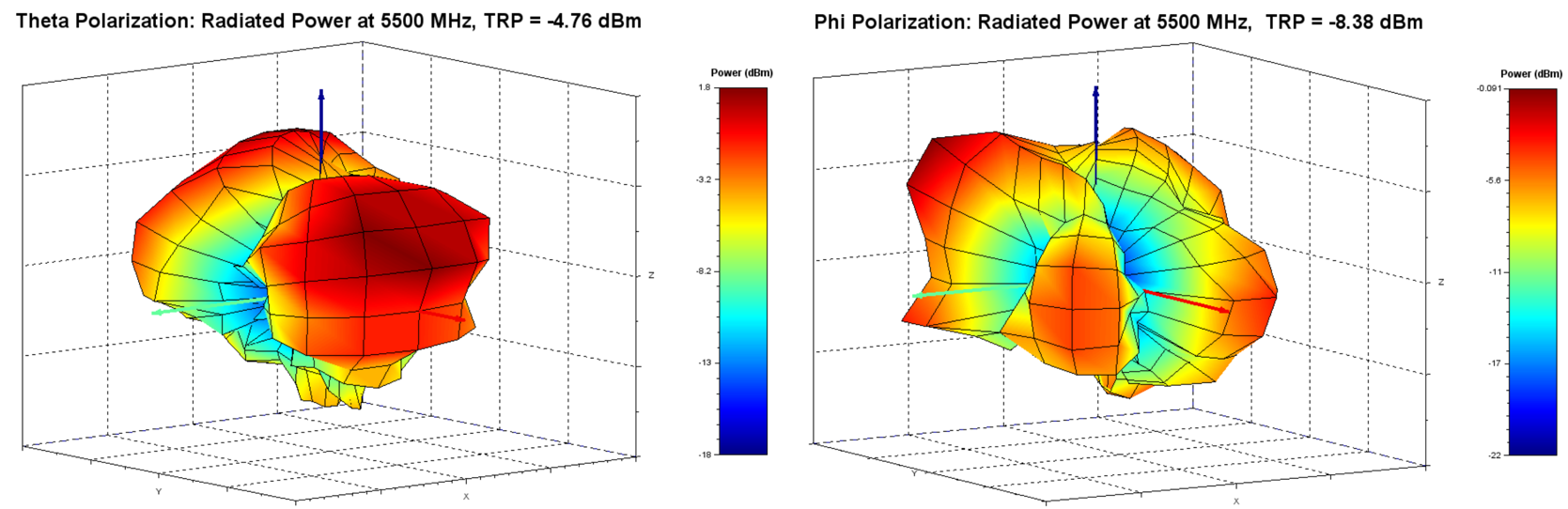
The patterns at other frequencies in the 5 GHz band exhibit the same radiated performance characteristics.
Ordering Information
| Part Number | Description |
|---|---|
| 453-00199R | Module, Sona TI351, 1216, MHF4L, Tape and Reel |
| 453-00199C | Module, Sona TI351, 1216, MHF4L, Cut Tape |
| 453-00200R | Module, Sona TI351, 1216, Chip Antenna, Tape and Reel |
| 453-00200C | Module, Sona TI351, 1216, Chip Antenna, Cut Tape |
| 453-00209 | Module, Sona TI351, M.2, Key E, MHF4L, SDIO, UART |
| 453-00200-K1 | Development Kit, Module, Sona TI351, Chip Antenna, SDIO, UART |
Revision History (Legacy)
| Version | Date | Notes | Contributors | Approver |
|---|---|---|---|---|
| 0.1 | Aug 20 2024 | Preliminary release | Dave Neperud | Andy Ross |
| 0.2 | Sep 19 2024 | Added shipping and labelling information for M.2 1216 module. Updated radio current values. | Dave Neperud | Andy Ross |
| 1.0 | Nov 5 2024 | Initial release. Corrected UART pin out and COEX pin out to the M.2 standard. Added shipping and label information for the M.2 2230 module. | Dave Neperud | Andy Ross |
| 1.1 | Feb 28 2025 | Additional implementation guidance on the SDIO_WAKE#/HOST_WL_IRQ line of the M.2 1216 modules in sections 5.1, 5.2, and 12.1 | Dave Neperud | Andy Ross |
| 1.2 | May 6 2025 | Added Product Notice at beginning of guide. | Dave Drogowski | Andy Ross |
| 1.3 | Nov 18 2025 |
| Connie Lin | Andy Ross |
Additional Information
Please contact your local sales representative or our support team for further assistance:
| Headquarters | Ezurio 50 S. Main St. Suite 1100 Akron, OH 44308 USA |
| Website | http://www.ezurio.com/ |
| Technical Support | http://www.ezurio.com/resources/support |
| Sales Contact | http://www.ezurio.com/contact |
Note: Information contained in this document is subject to change.
Ezurio’s products are subject to standard Terms & Conditions.